
With the contribution of researchers from the HUN-REN Wigner Research Centre for Physics, a study published in Nature Communications points to a new direction in the development of room-temperature quantum sensors and quantum communication devices based on two-dimensional materials.
Hexagonal boron nitride (hBN)—a two-dimensional, atomically thin crystal—has become a host for single-photon emitters (SPEs) and quantum defect spins that work even at room temperature. But despite impressive demonstrations, a central mystery lingered: What exactly are the atomic defects responsible for the different colors, lifetimes, and stability seen from one emitter to the next? And why do some centers show optically detected magnetic resonance (ODMR), the key to reading out quantum defect spins with light, while others do not?
In this work, Song Li, Anton Pershin, and Ádám Gali answer these questions by shifting the perspective from single, isolated defects to donor–acceptor pairs (DAPs)—two nearby defects that exchange charge and interact magnetically. Using ab initio (first-principles) simulations, they show that much of the diversity observed in hBN’s optical spectra can be explained if a common acceptor defect is paired with different donor partners at different separations. Specifically, the study identifies an oxygen substituting nitrogen next to a boron vacancy (denoted ON–VB, or ONVB) as the acceptor and shows that carbon substituting boron (CB) or oxygen substituting nitrogen (ON) defects can act as donors. The donor transfers an electron to ONVB, creating a negatively charged acceptor that emits light with properties that depend sensitively on the donor type and the donor–acceptor distance.
This pair-based picture neatly explains why some emitters in hBN have short or long lifetimes, why their zero-phonon line (ZPL) energies vary (often near ~2 eV), and why the brightness and stability differ from spot to spot—without invoking many unrelated defect species. For example, ON–ONVB pairs are predicted to be photostable with quantum yields comparable to the isolated ONVB, whereas certain CB–ONVB configurations create metastable “dim” states that open non-radiative decay channels and reduce brightness. The team further shows how external magnetic fields can activate an ODMR signal from an S = 1/2 ground state through hyperfine-mediated processes in these spin-pair systems—revealing a microscopic route to spin polarization and optical readout in hBN.
Why it matters?
First, the work provides a unifying framework for interpreting the patchwork of optical signatures reported across labs: many “different” emitters may actually be the same acceptor paired with different donors at different distances. Second, it offers a practical recipe for engineering better quantum devices: by controlling dopants and pair separations, researchers can tune color, lifetime, and spin-readout contrast—key steps toward indistinguishable photons and scalable quantum photonics in 2D materials. Finally, the paper clarifies when and how ODMR can arise in hBN from coupled spin pairs, guiding efforts to build robust room-temperature quantum memories and sensors.
The bigger picture. Identifying the atomic origin of SPEs is notoriously hard in 2D crystals, where local strain, fields, and buried layers complicate microscopy. By combining detailed electronic-structure theory with known EPR and microscopy evidence, the authors show that pair interactions of defects—not just isolated defects—play a central role in hBN’s quantum optics. That insight should accelerate deterministic fabrication and performance optimization of quantum emitters across the wide-band-gap materials family.
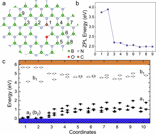
Figure: Point defect pairs are shown: (a) the red sphere (an oxygen-vacancy defect) and the brown sphere (a carbon atom substituting for a boron atom), where the carbon atom is placed at increasing distances, with the positions indicated by numbers. As a function of this separation, we present (b) the emission energy (ZPL energy, which determines the emission color) and (c) the corresponding electronic structure. We observe that the emission color depends on the distance between the two point defects.
